The light measurement technology has evolved during the years from the old traditional film based photography to one where electronic images are the choice. The imaging recording device is one of the most critical components so understanding the process of how the light images are recorded can increase the quality of the light measurement data.
© Copyright 2010 www.spacealliance.ro
The light measurement technology has evolved during the years from the old traditional film based photography to one where electronic images are the choice. The imaging recording device is one of the most critical components so understanding the process of how the light images are recorded can increase the quality of the light measurement data.
Although the charge-coupled device detector functions in an equivalent role to that of film, it has a number of superior attributes for imaging in many applications mentioning only extraordinary dynamic range, spatial resolution, spectral bandwidth, and acquisition speed.
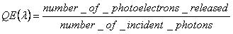
But the most important attribute, the quantum efficiency of a sensor is defined as:
a measure which is strongly depending of the

wavelength of the incident light.
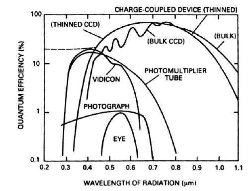
Next diagram shows why the CCDs or “charge couple devices” have been chosen as prime sensors. It clearly shows the QE has the highest value and is covering a large wavelength region.
A CCD is an array of small sensing elements called pixels and is built on the semiconductor technology which will be explained in the following section.
In general electrons from atoms have discrete energy levels but when the atoms come together forming a crystal structure the atoms interact and the upper energy levels of neighboring atoms start to share the electrons such that they create 3 so called bands:
-“valence bands” completely filled
-a “band gap” defined by

-“conduction bands” which are partially filled or empty and can be occupied by thermally activated electrons
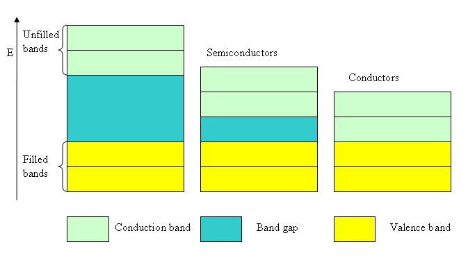
The characteristics of these bands split the materials between:
-metals in which case the band gap does not exist which means the valence and conducting band overlap. Because of this the metals have a high electric conductivity
-insulators in which case the band gap is wide and the electrons from the valence band cannot escape to the conductivity band leaving it empty. Because of this the insulators have no connectivity at all
-semiconductors in which case the band gap is sufficient narrow permitting to a significant number of electrons thermally excited to leave the position on the valence band and to pass to the conductivity band. Once reaching the conductivity band they can establish an electrical current under the action of an electric field.
The holes left in the valence band give possibility to other valence electrons to move around and occupy the empty positions contributing to the electric conductivity under the “electron hole pairs” effect.
There are several preferred materials for semiconductors and the following diagram lists their characteristics.
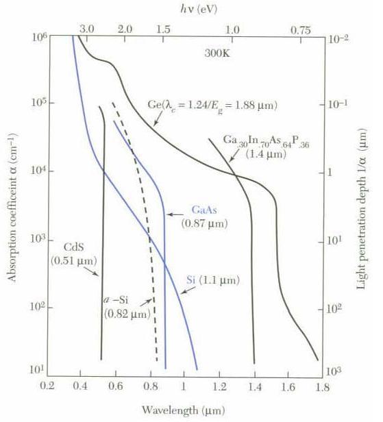
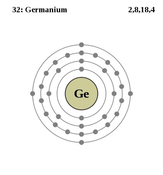
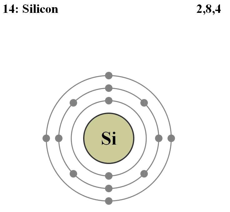
The most common materials are Ge and Si. They have both 4 valence electrons and are “intrinsic photoconductors” which means that a single optical infrared photon is sufficient to excite their electrons to the conduction band where they can migrate through the crystal and later amplified by applying an electric field to the crystal.
The process of photo absorption in semiconductor material depends directly of the wavelength of the incident photon by the following formula where the photon flux

at a certain depth

in the material depends on the absorption coefficient

:

The absorption coefficient as it can be seen from the above diagram has lower values for higher wavelengths and higher values for lower wavelengths, which from the physical aspect means “redder” photons can propagate deeper in the semiconductor crystal before being absorbed than those “bluer” and in the same time making harder to give to the valence electrons enough energy to overcome the band gap.
This phenomenon is known as the red wavelength limit for semiconductors, a cut off energy where no light is absorbed by the crystal any longer.
The value of the cut off wavelength for a given semiconductor is given by:

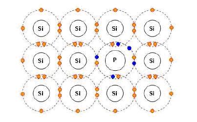
In order to increase the natural sensitivity limit of the semiconductor material a doping process is used in the industry which basically means creating a so called “extrinsic photoconductors” by adding some impurities to the semiconductor and thus creating charge carriers by exciting electrons from doped atoms into the conduction band.
Based on the number of valence electrons from the doped atom compared with the number of valence electrons from the semiconductor there are two types of photoconductors resulting:
-a “n-type” semiconductor when the number of valence electrons from the doped atom exceeds the number of valence electrons from the native semiconductor material
-a “p-type” semiconductor when the number of valence electrons from the doped atom is less than the one from the native material semiconductor
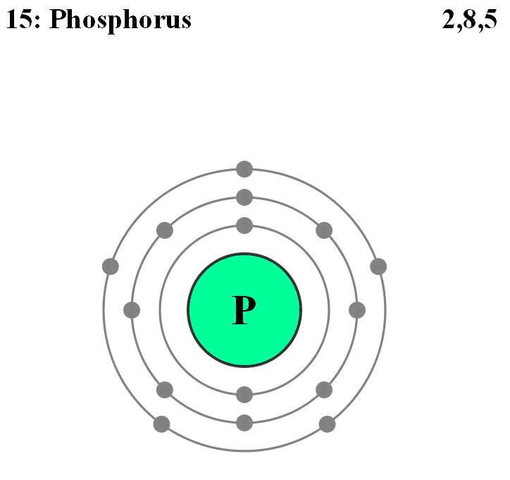
A typical case is the one of Si photoconductors doped as “p-type” semiconductors using a P atom.
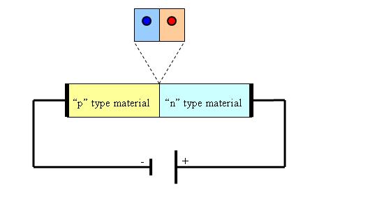
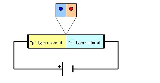
When two “n-type” and “p-type” semiconductors are put into contact it results a “p/n junction” where will take place diffusion of holes into the n-type material and respectively diffusion of electrons into the p-type material. However the depletion zone which takes place at the junction between them is a non-conducting layer because the electrical carriers from both sides attract and eliminate each other under the recombination process.
Without an external applied voltage an equilibrium condition is reached described by the built in potential across the junction. In equilibrium p-n junction electrons near the p-n interface tend to diffuse into the p region leaving the positive charged ions called donors in the n region. In a similar way holes near the p-n interface begin to diffuse into the n-type region leaving fixed ions called acceptors with negative charge. Therefore the regions nearby the p-n interface lose their neutrality and become charged forming the space charge region or depletion layer.
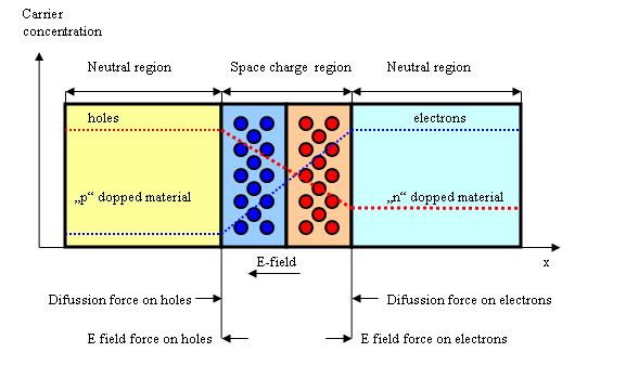
Next diagram shows how the two processes work and how the equilibrium is reached-on one side the diffusion process that is generating more space charge and on the other side the electric field generated by the space charge region opposes the diffusion.

If a positive voltage is applied to the n-type material and a negative voltage is applied to the p-type material, the junction will become conductive in the moment when the voltage surpasses the barrier causing the “forward bias” effect.
By contrary when a positive voltage is applied to the p-type material and a negative voltage is applied to the n-type material the diffusion process increases leading to a depletion of positive charge carriers in the n-type material and to negative charge carriers to the p-type material, the final effect being the increasing of the depletion region. This is called the “reverse bias” effect.